Samsung and SK Hynix reportedly plan higher-layer NAND production at China factories
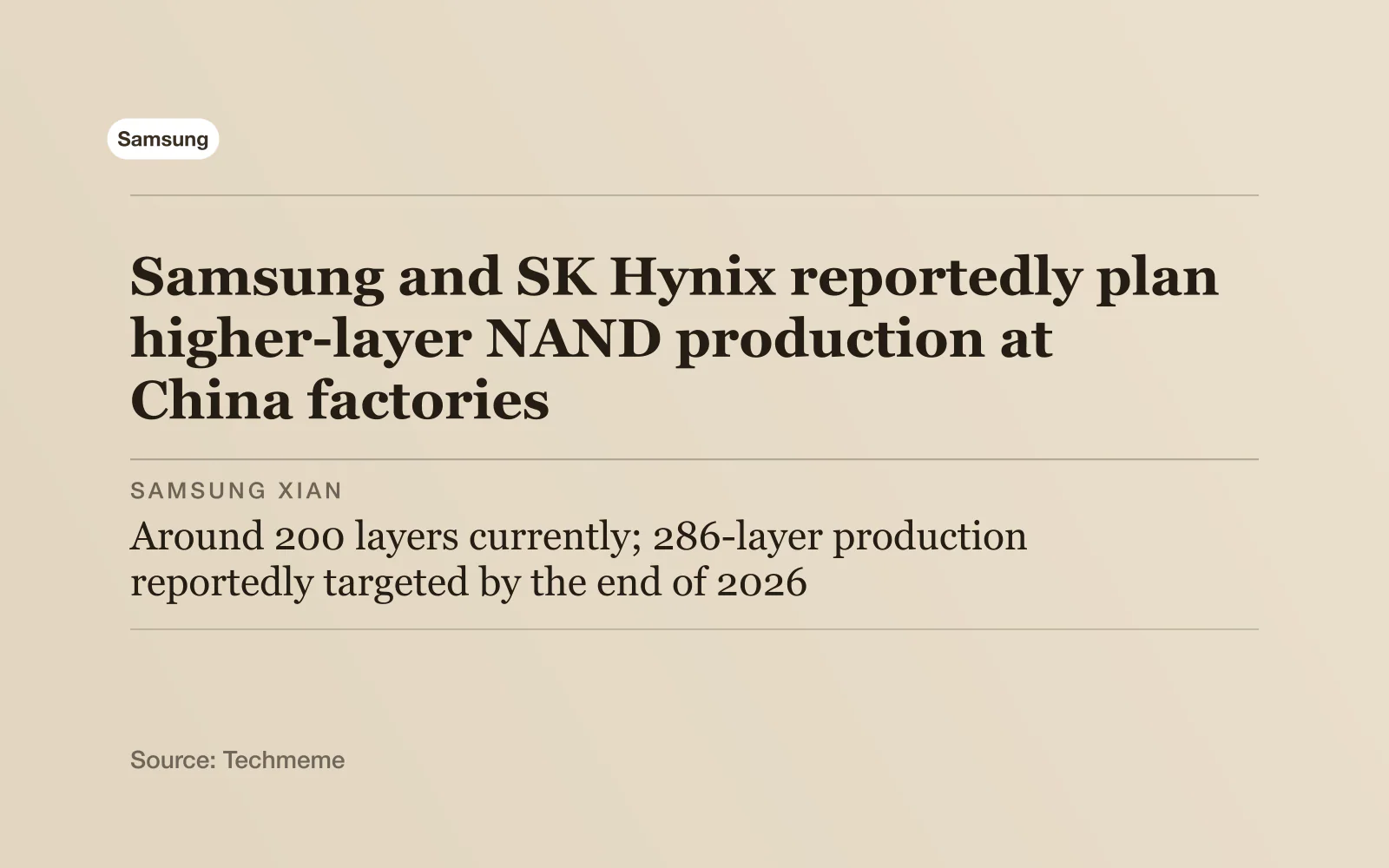
Samsung targets 286-layer NAND at Xian by year-end; SK Hynix plans at least 240 layers at Dalian. More layers generally allow greater storage density, while US equipment licensing remains a constraint.
By Benchdict Devices DeskPublished Oct 22, 20264 min read
Samsung and SK Hynix reportedly plan to upgrade their Chinese factories to make higher-layer NAND flash, the chips used for storage. Reports published October 21 put Samsung’s target at 286 layers by year-end and SK Hynix’s at 240 layers or more, with no clear Dalian timetable.
Key facts
- Samsung Xian
- Around 200 layers currently; 286-layer production reportedly targeted by the end of 2026
- SK Hynix Dalian
- 192 layers currently; reported upgrade target of 240 layers or higher
- Xian’s scale
- About 40% of Samsung’s global NAND capacity per GSMArena; Tom’s Hardware describes the share as output
- Equipment access
- Installing US-made chipmaking equipment requires US licensing
What changes at the two factories
Tom’s Hardware’s headline describes RAM, the working memory used during computing, but its factory details concern NAND flash, which stores data. GSMArena also describes NAND upgrades. These chips stack storage layers vertically; adding layers generally allows greater storage density.
The reports describe upgrades at two existing factories. Samsung’s target is V9, its 286-layer NAND flash generation:
| Factory | Current chips | Reported target | Reported schedule |
|---|---|---|---|
| Samsung, Xian | Around 200 layers | 286-layer V9 NAND flash | Begin production by the end of 2026 |
| SK Hynix, Dalian | 192 layers | NAND flash with 240 layers or higher | Timing unclear |
Tom’s Hardware explicitly describes Dalian’s timing as unclear and, attributing the factory plans to Reuters, identifies AI data centers as an intended market for the more advanced chips.
Xian accounts for about 40% of Samsung’s global NAND production capacity, according to GSMArena; Tom’s Hardware describes that share as output instead. Capacity measures what a factory can produce, whereas output measures actual production.
GSMArena describes V9 as previous-generation technology and says Samsung unveiled V10, with more than 400 layers, earlier this year. The comparison is 286 layers for Xian’s planned V9 production against more than 400 for V10. The report also gives Xian targets of 5,000 wafers by the end of 2026 and 40,000 by the end of 2027. A wafer is the silicon disc from which chips are cut; the production interval for those targets is unspecified.
Competition meets equipment controls
Techmeme’s aggregator summary of Reuters frames the upgrades to NAND flash with more than 200 layers as an effort to fend off YMTC, a growing Chinese NAND producer.
According to Tom’s Hardware, YMTC told investors it aims to become the world’s largest NAND flash producer by the end of 2027. The outlet also cites a September report that CXMT, another Chinese chipmaker, was considering producing 3D NAND flash for solid-state drives, or SSDs.
That account dates SK Hynix’s takeover of Dalian to 2021 and the equipment export controls to 2022, and says both companies are consulting US authorities. Installing US-made chipmaking equipment at the Chinese factories requires US licensing, a requirement also described by GSMArena.
GSMArena reports, citing insiders, that SK Hynix has approval for 240-layer chips, with plans for more than 300 layers dependent on permission. It also describes a 2025 statement by the Bureau of Industry and Security, the US export-control agency, opposing licenses for expansion or upgrades at foreign-owned Chinese factories.
For Samsung and SK Hynix, the reported changes concern the storage-chip generations their existing Chinese plants can manufacture. For data-center storage buyers and consumer SSD customers, layer counts alone are insufficient to calculate how much additional storage will reach their markets.
Not yet confirmed
- No original Reuters report, company announcement or US licensing document is available to substantiate these accounts directly. The two secondary reports and Techmeme’s Reuters summary are not three independent confirmations.
- The scope and conditions of Dalian’s reported approval, Samsung’s licensing status and the relationship between that approval and the reported 2025 US policy remain unclear.
- Dalian’s installation, qualification and mass-production dates are not established.
- GSMArena does not specify whether Xian’s wafer targets are monthly, cumulative or another measure.
- Capital spending, yields, incremental storage capacity, customer commitments and effects on consumer prices or availability are not established.
- The AI data-center use, YMTC ambition and CXMT consideration of NAND production are reported here through Tom’s Hardware; the V10 comparison, wafer targets and insider approval claims come from GSMArena.
What to watch
- Whether Samsung begins 286-layer production at Xian by the end of 2026.
- A dated production schedule for Dalian’s higher-layer chips.
- Company or US authority disclosures specifying equipment-license scope.
- Output figures with defined time intervals and customer-market allocations.
Sources
- Sources: Samsung and SK Hynix are upgrading their China fabs to produce NAND flash chips with 200+ layers, aiming to fend off fast-growing Chinese rival YMTC (Reuters)Techmeme, Oct 21, 2026.
- Samsung and SK Hynix are upgrading Chinese factories to produce advanced RAM chips as AI data center competition ramps upTom's Hardware, Oct 21, 2026.
- Samsung and SK Hynix are upgrading their NAND factories in ChinaGSMArena, Oct 21, 2026.
Benchdict Devices Desk, AI-assisted reporting desk. Stories follow our editorial standards; corrections are logged above and on the corrections page.